FPGAs
Field-Programmable Gate Arrays (FPGAs) are versatile integrated circuits that offer immense flexibility in digital circuit design. Unlike traditional Application-Specific Integrated Circuits (ASICs), FPGAs can be reconfigured after manufacturing, making them ideal for a wide range of applications. Let’s delve into the intricacies of FPGAs:
1. The Basics: What Are FPGAs?
- Definition: FPGAs are semiconductor devices that allow you to create custom digital circuits by configuring their internal resources.
- Logic Blocks: An FPGA consists of an array of programmable logic blocks. Each block contains a collection of logic gates (such as AND, OR, NOT) that can be interconnected to implement complex functions.
- Switch Matrix: The heart of an FPGA is its switch matrix. This matrix allows you to connect various logic blocks together, forming the desired circuit.
and can be connected together using the switches inside the chip. To program a fpga you’ll need to create a bitstream file. The bitstream file will contain the memory configuration and connections.
2. How FPGAs Work: A Closer Look
- Memory Locations: FPGAs contain memory locations (known as configuration cells) that store the logic configuration. These cells determine how the logic blocks are interconnected.
- Switches: The switches inside an FPGA control the connections between logic blocks. By setting the switches, you define the circuit’s behavior.
- Inputs and Outputs: Each logic block has inputs and outputs. These correspond to the inputs and outputs of the logic gates within the block.
- Routing Resources: FPGAs also provide routing resources (wires and interconnects) that allow signals to flow between logic blocks.
3. Programming an FPGA: The Bitstream File
- Bitstream: To program an FPGA, you create a bitstream file. This file contains the configuration information for the FPGA.
- Memory Configuration: The bitstream specifies which logic blocks are active, how they are interconnected, and the values stored in their memory locations.
- Tools and Languages: You can use specialized software tools (such as Xilinx Vivado or Intel Quartus) to generate the bitstream. These tools allow you to describe your circuit using Hardware Description Languages (HDLs) like VHDL or Verilog.

Programming with F4PGA
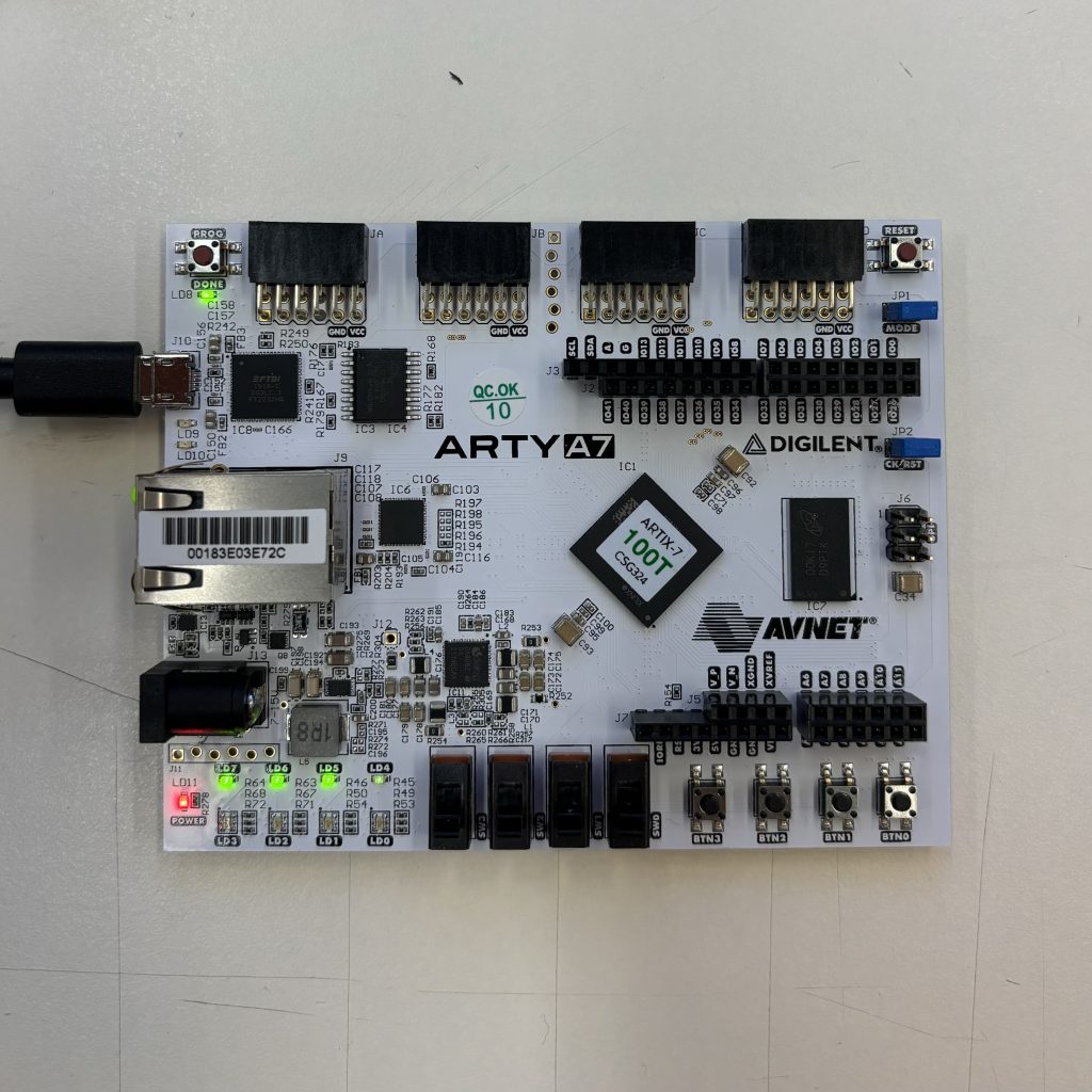
In the hackerspace we have a couple ARTY A7 100s. These chips are pretty powerful and allow you to simulate an entire risc-v core. However, we will be looking at the basic workflow and how program these fpgas using a simpler program.
Step one – Installation
Go to F4PGA to install the toolchain. The tool chain is a collection of tools which help us create and deploy the bitstream to the fpga.
Follow the following article to install the toolchain.
Getting F4PGA — F4PGA examples documentation (f4pga-examples.readthedocs.io)
Note: Make sure to choose the ARTIX-7 Family when installing the packages. This is the FPGA chip on the arty.
Step Two – Connect Arty
Use a USB micro-b cable to connect the Arty to your computer. A light will illuminate when the arty is connected.
Note: arty has two flashing modes
There’s a jumper cable near the top of the arty which allows selections of flash mode or rom mode.
Flash mode (jumper in) – Will load the program in memory. The program doesn’t remain on the arty after it’s shut off.
ROM mode (jumper out) – Will load the program into ROM. The program will remain on the arty after it’s shut off.
Step Three – Flash Arty
If you followed the steps on the F4PGA for setting up the environment. The next step is to create a program. F4PGA gives example programs like the counter_test to flash. Simply cd into xc7 directory and type the following command
TARGET=”arty_100″ make download -C counter_test
This will set the Target as arty 100 and flash the board using openFPGALoader.
